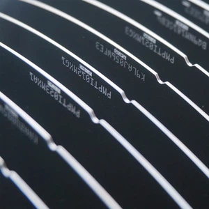
Cia peb ua ib qho 4-inch monocrystalline silicon wafer ua piv txwv:

Raws li qhia saum toj no:
Kev taw qhia: <100>qhia txog crystallographic orientation ntawm silicon wafer. Qhov kev taw qhia no muaj qhov cuam tshuam tseem ceeb rau cov khoom siv hluav taws xob thiab kev tsim khoom ntawm cov khoom siv ntawm lub wafer.
Hom:P (Boron) nrog ib lub tiaj tiaj txhais tau hais tias lub wafer yog P-hom silicon, uas yog, nws yog doped nrog boron los tsim qhov ntau dhau. "ib qho chaw tiaj tus" yog hais txog cov duab ntawm ntug ntawm lub wafer, uas yuav pab txheeb xyuas cov kev taw qhia ntawm cov siv lead ua lattice.
Kuj:1-10 Ohm-cm yog qhov resistivity ntawm wafer.
Qib:Prime / CZ Virgin qhia qhov zoo thiab purity ntawm silicon wafer. "Prime" yog qib siab tshaj plaws thiab yog siv rau cov ntawv thov siab; "CZ" yog hais txog ib leeg-crystal silicon wafers ua los ntawm CZ txoj kev.
Txheej:Tsis muaj, haiv neeg oxide tsuas yog txhais tau tias tsis muaj txheej txheej zaj duab xis ntxiv rau ntawm qhov chaw ntawm lub wafer, tsuas yog ib txheej txheej silicon dioxide.
Thickness:525µm (+/{2}}µm) yog lub thickness ntawm lub wafer, thiab qhov yuam kev yog tswj nyob rau hauv ntxiv los yog rho tawm 20 microns. Thickness uniformity yog qhov tseem ceeb rau cov kauj ruam tom ntej.
Txoj kab uas hla:100mm qhia txoj kab uas hla ntawm wafer.
Warp:<=30µm, the lower the warp, the better the wafer quality.
bowing: <=30µm, similar to warping, it is also a measure of wafer flatness.
Main positioning ntug:32. Qee cov wafers kuj muaj qhov chaw nruab nrab, raws li qhia hauv qab no:

Nto roughness:0.